Research topics
By skillfully utilizing nanostructures, heat transport phenomena that cannot occur at conventional scales become possible. Unknown physics remains in this domain, and we are advancing the exploration of heat transport physics in semiconductors and two-dimensional materials, as well as developing next-generation thermal flow control technologies. Additionally, we are researching new fundamental physics unique to hybrid states of multiple quanta that cannot be achieved with single types of quanta. Meanwhile, we are developing thermal management technologies for advanced semiconductors supporting the growth of the AI industry and environmental heat power generation technologies, creating energy-saving and energy-generating devices that contribute to carbon neutrality. Furthermore, using our proprietary three-dimensional thermal conductivity measurement and imaging techniques, we conduct thermal measurements and analyses of materials and devices such as graphene, AlN, and SiC, supporting thermal management essential for advanced semiconductors and power semiconductors. We are advancing research in the following areas: thermal management technologies for advanced semiconductor materials and devices, environmental heat power generation, phonon engineering, photo-thermal fusion projects, and quantum information networks using phonons. These efforts are promoted through multiple large-scale projects including JST’s Strategic Basic Research Programs, JST-Mirai Program, and Moonshot Research and Development Programs.
【Recent Invited Review Paper】M. Nomura, “Ubiquitous phonon engineering: Thermal phonon transport at the nanoscale,” JSAP Rev. 240210 (2024).
Keywords: Advanced semiconductors, thermal management, phonon engineering, phononic crystals, thermoelectric conversion, environmental power generation, energy harvesting, hybrid quantum science, quantum computer
Advanced semiconductor thermal management
Heat Dissipation Technology Supporting the Development of the AI Industry
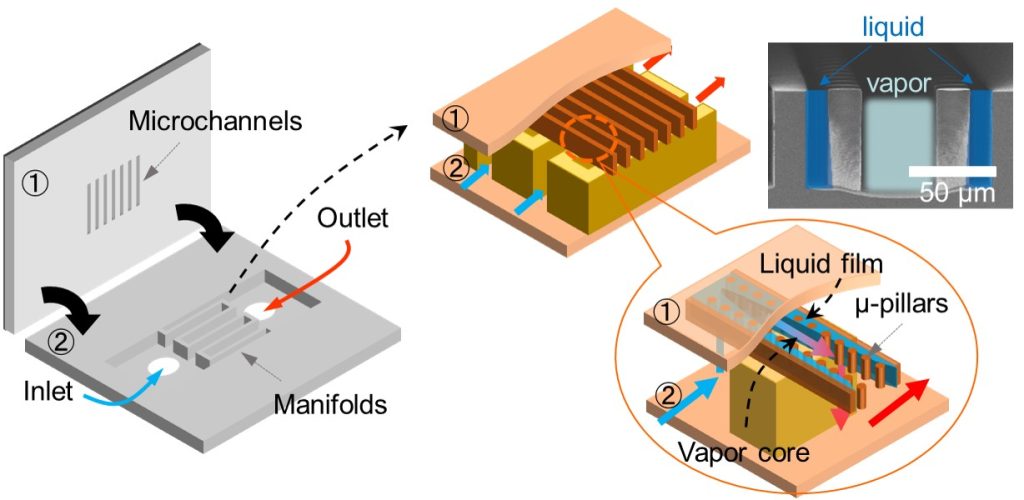
Advanced semiconductors are being developed toward three-dimensional structures that are faster and more energy-efficient. Since HBM (High Bandwidth Memory) is stacked directly on GPUs, improving heat dissipation technology is essential for enhanced performance. Our laboratory is conducting research on: Topic1 water cooling technology using three-dimensional microchannels and Topic2 realization of high heat dissipation semiconductor chips using AlN insulating films. Particularly for Topic1, we form microchannels inside silicon chips, inject a small amount of cooling water, and achieve semiconductor chip cooling at world-leading efficiency levels with a COP (Coefficient of Performance) exceeding 10^5 through two-phase cooling using the heat of vaporization from boiling.
References
- H. Shi, S. Grall, R. Yanagisawa, L. Jalabert, S. Paul, S. H. Kim, J. L. Viovy, H. Daiguji, and M. Nomura, “Chip cooling with manifold-capillary structures enables 105 COP in two-phase systems,” Cell Reports Physical Science 6, 102520 (2025).
- W.-Y. Woon, A. Kasperovich, J.-R. Wen, K. K. Hu, M. Malakoutian, J.-H. Jhang, S. Vaziri, I. Datye, C. C. Shih, J. F. Hsu, X. Y. Bao, Y. Wu, M. Nomura, S. Chowdhury, and S. Sandy Liao, “Thermal management materials for 3D-stacked integrated circuits,” Nature Reviews Electrical Engineering 2, 598, (2025).
Thermoelectric energy harvesting
More than half of the electric power generated in the world is wasted as heat energy. Almost all the electric and electronic devices are designed for low power consumption, but some of the supplied energy is lost as heat. Therefore, development of thermoelectric devices, which can convert the waste heat energy into electric energy, is highly expected. In the future, broad area sensor network will be constructed and enormous number of sensor nodes will be distributed to monitor, for example, the infrastructures. It is not so realistic to use batteries or wires to supply the electric power to the sensor nodes. Therefore, energy harvesting will be essential technology for energy autonomous. There are several energy conversion technology such as photovoltaic, thermoelectric, piezoelectric, and so on. Our group focuses on thermoelectrics.
Thermoelectric devices have many attractive advantages including high reliability stems from no moving parts, and maintenance free device. Therefore, this device is used for artificial satellite, for example. However, with the convenience, we do not find many thermoelectric devices around. There are two main reasons: the conversion efficiency stays only several % at present and the improvement in the efficiency is required before practical use. Moreover, the conventional thermoelectric materials contain hazardous heavy elements and low environmental load material will be welcome.
We collaborate with University of Freiburg in Germany to fabricate highly efficient Si thermoelectric devices and monitoring systems using both nanotechnology and micromachining technology.
References
- R. Yanagisawa, S. Koike, T. Nawae, N. Tsujii, Y. Wang, T. Mori, P. Ruther, O. Paul, Y. Yoshida, J. Harashima, T. Kinumura, Y. Inada, and M. Nomura, “High-power-density hybrid planar-type silicon thermoelectric generator with phononic nanostructures,” Mater. Today Phys. 45, 101452 (2024).
- S. Koike, R. Yanagisawa, L. Jalabert, R. Anufriev, M. Kurosawa, T. Mori, and M. Nomura, “Planar-type SiGe thermoelectric generator with double cavity structure,” Appl. Phys. Lett. 124, 123902 (2024).
Thermal phonon engineering:
Physics and applications of nanoscale heat transfer
Artificial control of the thermal conductivity is not only the important technology for thermoelectrics but also is an interesting topic in fundamental physics. Thermal conductivity is a unique physical parameter for a material. In non-doped silicon, phonons, quanta of the lattice vibration, are the main heat carriers. By forming thick nanowires or form nanocomposite in the structures, one can reduce the thermal conductivity due to increased surface and boundary scattering processes. These scattering processes can be understood by particle picture of a phonon. We are interested in phonon transport control using ballistic characteristic of phonons (Ray phononics). On the other hand, manipulation of phonon transport by phononics, which is based on the band engineering is possible. This technique is based on the wave picture of phonons. In bulk material, the phonon transport (heat transfer) is described by Fourier law with diffusive process. However, when the dimension of the system comes down to mesoscale, where the size of the system is comparable to the mean free path of phonons, the phonon transport will be ballistic, and the physics will not follow Fourier law.
We investigate phonon transport in Si nanostructures, which is a key to higher conversion efficiency, with a dimension below 100-nm fabricated by top-down lithographic technology. We design phononic crystal structures, which can control phonon transfer while preserving good electric conductivity. We originally developed micro time-domain thermoreflectance system, which can measure thermal conductivity of nanostructures with very high throughput. We found that thermal conductivity in a one-dimensional phononic crystal is largely reduced compared with the value for nanowires with similar width.
We have also developed a Phonon Monte Carlo algorithm that simulates ballistic transport of phonons, and have released it as a free and open-source python application FreePATHS. It is expected to increase the degree of freedom in controlling heat conduction in solids and help solve the problem of heat dissipation.
References
- X. Huang, R. Anufriev, L. Jalabert, K. Watanabe, T. Taniguchi, Y. Guo, Y. Ni, S. Volz, and M. Nomura, “A graphite thermal Tesla valve driven by hydrodynamic phonon transport,” Nature 634, 1086 (2024).
- B. Kim, F. Barbier–Chebbah, Y. Ogawara, L. Jalabert, R. Yanagisawa, R. Anufriev, and M. Nomura, “Anisotropy reversal of thermal conductivity in silicon nanowire networks driven by quasi-ballistic phonon transport,” ACS Nano 18, 10557 (2024).
- M. Nomura, R. Anufriev, Z. Zhang, J. Maire, Y. Guo, R. Yanagisawa, and S. Volz, “Review of thermal transport in phononic crystals,” Mater. Today Phys. 22, 100613 (2022). (Invited review)
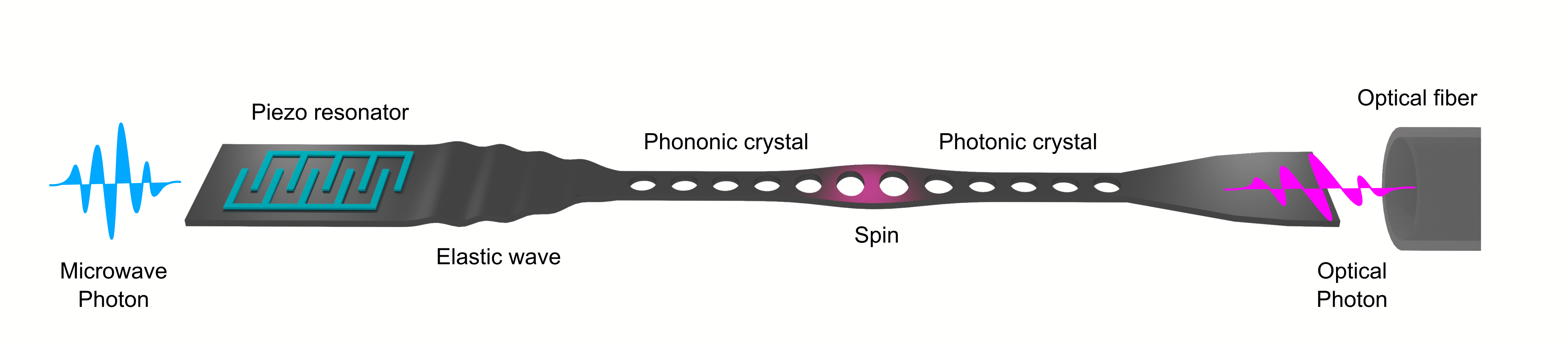
Phonon hybrid quantum science
The purpose of this research is to demonstrate the surface wave mediated heat conduction, namely how we can improve the heat dissipation in submicron thin films. Over the past decade, significant research efforts have been devoted to the study of these surface waves, because the surface effects predominate over the volumetric ones in nanostructures with high surface-to-volume ratio. Some types of surface electromagnetic waves may even carry heat and thus improve the thermal performance and stability of nanoscale devices. One type of such surface waves is the surface phonon-polariton (SPhP), which occurs as a hybrid of optical phonons and surface electromagnetic waves. The SPhP are essentially evanescent waves that propagate along the surface of polar dielectric membranes. Nevertheless, the experimental demonstration of SPhP contribution to in-plane thermal conductivity in nanofilm is lacked to date.
In our study, we experimentally measured the in-plane thermal conductivity of amorphous SiN membranes at different temperatures. A significant increase of the thermal conductivity with temperature in the 300 – 800 K range has been observed for membranes thinner than 50 nm. We attribute this enhancement to the propagation of surface phonon-polaritons along the membrane interfaces. Our results demonstrate that the reduction of the phonon thermal conductivity of nanomaterials can be compensated by the increase of its counterpart driven by the propagation of surface phonon-polaritons and even double the thermal energy transport. Thus, this work uncovers a new channel of heat transport along polar dielectrics and lays the foundations for improving the heat dissipation in microelectronics and efficiency in silicon photonics.
Reference
- S. Tachikawa, J. Ordonez-Miranda, L. Jalabert, Y. Wu, R. Anufriev, Y. Guo, B. Kim, H. Fujita, S. Volz, and M. Nomura, “Enhanced far-field thermal radiation through a polaritonic waveguide,” Phys. Rev. Lett. 132, 186904 (2024).
- Y. Wu, J. Ordonez-Miranda, S. Gluchko, R. Anufriev, D. De Sousa Meneses, L. Del Campo, S. Volz, M. Nomura “Enhanced thermal conduction by surface phonon-polaritons” Science Advances 6, eabb4461 (2020).
Fundamental study of heat conduction
※ Invited Review Review of thermal transport in phononic crystals
Research of our theoretical subgroups focuses on the atomistic modeling of nanoscale thermal transport and thermoelectric energy conversion properties of nano-materials and nanostructures. We are using methodologies for nanoscale thermal transport study, such as molecular dynamics simulations, ab-initio calculation, and atomistic non-equilibrium green’s function. Right now, we are working on the characterization of modal particle- and wave-like/coherent behavior of thermal phonons in low-dimensional systems. Based on the definition of phonon wavepacket, recently we proposed a new model to quantifying the intrinsic coherence of thermal phonons, which has a general impact on the estimation of the thermal properties in nanostructures as well as in bulk materials.
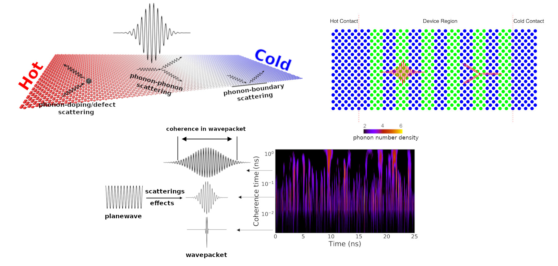
Moreover, we are working on the quantum/coherent nature and transport of phonons in nanophononic structures and at interface, anharmonic phonon non-equilibrium Green’s function (NEGF) formalism and application and mesoscopic modeling of phonon hydrodynamic transport.
References
- W. Zhang, X. Xiong, Y. Guo, H. Yi, S. Volz, M. Nomura, “Promoting Anderson Localization for Low-Frequency Phonons in SiGe Alloyed Nanowires with Long-Range Correlated Disorder,” ACS Nano 19, 37004 (2025).
- X. Huang, R. Anufriev, L. Jalabert, K. Watanabe, T. Taniguchi, Y. Guo, Y. Ni, S. Volz, and M. Nomura, “A graphite thermal Tesla valve driven by hydrodynamic phonon transport,” Nature 634, 1086 (2024).
- X. Wu, X. Huang, L. Yang, Z. Zhang, Y. Guo, S. Volz, Q. Han, and M. Nomura, “Suppressed thermal transport in mathematically inspired 2D heterosystems”, Carbon 213, 118264 (2023).
- X. Huang, Y. Guo, Y. Wu, S. Masubuchi, K. Watanabe, T. Taniguchi, Z. Zhang, S. Volz, T. Machida, and M. Nomura, “Observation of phonon Poiseuille flow in isotopically purified graphite ribbons”, Nat. Commun., 14, 2044 (2023).
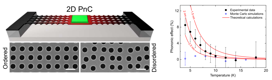
Thermal phononics
Heat flow is transport of ensemble of phonons in condensed matters. Thermal transport in nanostructures is in semi-ballistic regime and thus, it is largely different from that described by diffusive transport in bulk material. In a system with its characteristic length comparable to phonon coherence length, wave nature of phonons becomes important as well as particle nature. We aim to control thermal conduction by the use of the wave nature of phonons with phononic crystal nanostructures and investigate phononics. We design phononic crystal nanostructures by simulating phononic band diagrams and power flux for various structures. Our experiments demonstrated to control thermal transport at low temperature using phonon interference in phononic crystals.
References
- M. Diego, J. Hardouin, G. Mazevet-Schargrod, M. Pirro, B. Kim, R. Anufriev and M. Nomura, “Hypersonic acoustic wave control via stealthy hyperuniform phononic nanostructures,” Science Advances 11, 32, (2025).
- J. Maire, R. Anufriev, A. Ramiere, R. Yanagisawa, S. Volz, and M. Nomura, “Heat conduction tuning by wave nature of phonons,” Science Advances 3, e1700027 (2017)
Optomechanics
In nanoscale systems, the motion of the structure can be controlled by momentum of photons and optical gradient force. We investigate optomechanical coupling between the motion of GaAs semiconductor membranes and cavity photons, which is strongly localized in a high-Q photonic crystal nanocavity. The optomechanical systems are fabricated using electron beam lithography and reactive ion etching on a GaAs semiconductor wafer. The device performance is evaluated by a near infrared photoluminescence spectroscopy system with a wavelength tunable semiconductor laser.
This device is designed to have strong optomechanical coupling in the 1.55 um-optical communication band. We evaluate the mechanical and optical properties, and controllability of mechanical motion to optimize the optomechanical coupling in this system by using commercial and our simulators. We designed and fabricated GaAs-based optomechanical systems with the strongest optomechanical coupling using nanocavity. The goal of this research topic is demonstration of unique functional devices using integrated quantum systems.
References
- B. Kim, H. Kurokawa, K. Sakai, K. Koshino, H. Kosaka, and M. Nomura,” Diamond optomechanical cavity with a color center for coherent microwave-to-optical quantum interfaces,” Phys. Rev. Appl. 20, 044037 (2023).